Who is winning The Great Yield Wall? Beneath the veneer of the Chip 4 Alliance lies a brutal bidding war for the future of silicon. Washington triggered a techno-nationalist arms race among its closest allies — and it is already losing. But the real winner may not be any nation-state at all.
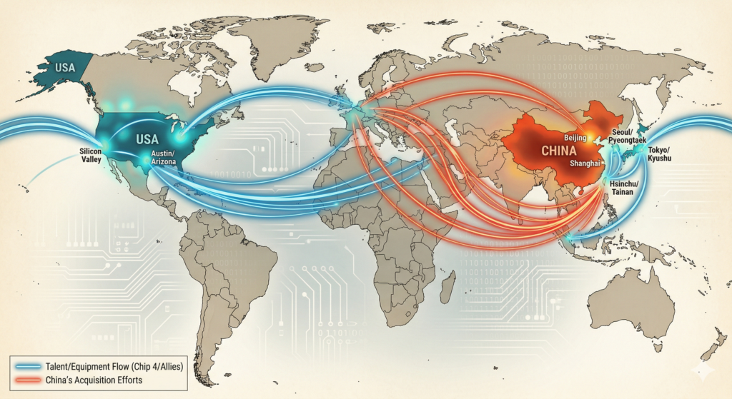
A heat map of the world showing the “Chip 4” nations (USA, Japan, South Korea, Taiwan) and China, with lines representing the flow of talent and equipment.
Semiconductor Industrial Policy (Q1 2026)
| Metric | Region/Entity | Program & Context | Strategic Impact |
| ¥10T (~$65B) | Japan | Rapidus Commitment (through 2030) | A “Kamikaze bet” to skip three nodes and hit 2nm by 2027. |
| $450B | South Korea | K-Semiconductor Strategy (Public + Private) | Building a 200-mile “K-Belt” to vertically integrate the supply chain. |
| ~15% | USA | CHIPS Act Disbursement (to date) | Highlights bureaucratic friction; compares poorly to 86%+ for Rapidus. |
| 31% | China | Global 28nm Capacity Share (Projected 2027) | The “Legacy Trap”—dominating the world’s nervous system while allies fight over the brain. |
Picture two rooms, both in the business of building the future. In one, Washington bureaucrats process CHIPS Act grant applications — reviewing childcare provisions, Davis-Bacon labor compliance, environmental impact statements, profit-sharing disclosures.
In the other, an engineer in Chitose, Hokkaido watches the world’s most advanced lithography machine fire its first laser — just three months after it arrived at the airport, a timeline with no known precedent anywhere else on earth.
Both rooms believe they are winning the most important industrial race of the century. Only one is moving at the speed the race demands. And neither may ultimately determine who wins it.
The CHIPS and Science Act
The CHIPS and Science Act of 2022 was Washington’s declaration of war on the semiconductor status quo — a $52 billion commitment to bring chip manufacturing back to American soil after decades of offshoring. It was bipartisan, historic, and strategically necessary. It was also, in the unsparing arithmetic of techno-nationalism, deeply underpowered relative to what America’s two closest Asian allies were simultaneously assembling.
Japan pledged roughly ¥10 trillion (~$65B) through 2030 and handed a state-backed startup the keys to a 2-nanometer fab with instructions to be operational by 2027. South Korea mobilized a $450 billion public-private semiconductor strategy, announced a 200-mile industrial corridor from Seoul to Busan, and began subsidizing corporate infrastructure costs the CHIPS Act explicitly refuses to cover.
Neither government burdened its program with childcare mandates, environmental review timelines, or union arbitration requirements. Neither is currently subject to a presidential demand for its abolition.
The Alliance That Became a Bidding War
The uncomfortable truth at the heart of the Chip 4 Alliance — the U.S.-Japan-South Korea-Taiwan coordination framework built to counter China’s semiconductor ambitions — is that it has become a structure within which allies compete ruthlessly for the same engineers, the same equipment suppliers, the same leading-edge customers.
This is not a failure of the alliance. It is its natural consequence. When governments inject hundreds of billions into a sector, they do not create cooperation. They create a zero-sum bidding war with diplomatic paperwork stapled to the front.
The Chip 4 Alliance was designed as a unified front against China. It has become a structure within which allies cannibalize each other’s supply chains while maintaining the diplomatic fiction of coordination.
What follows is a war room assessment. The story is more complicated than either Washington’s boosters or its critics allow. But the strategic verdict, when examined with investor-grade skepticism, is harder to contest than it should be.
The Theatre of Operations Setting the Battlefield
Semiconductors are not a product category — they are the substrate of every strategically significant technology of the next three decades: artificial intelligence, autonomous weapons, quantum computing, advanced communications.
Every GPU training a large language model runs on advanced chips. Every satellite navigation system, every electronic warfare suite, every next-generation fighter jet depends on process nodes measured in single-digit nanometers. Whoever controls the fabrication of those nodes controls the commanding heights of 21st-century power.
Silicon as the New Strategic Commodity
This is the logic of resource mercantilism applied to silicon. Nations are not merely competing for market share; they are hoarding strategic production capacity, building redundant domestic supply chains not because market economics demands it but because geopolitical risk calculus does.
The result is a global chip industry being pulled apart at the seams by competing national security imperatives, each backed by sovereign treasuries willing to absorb losses no private market would tolerate.
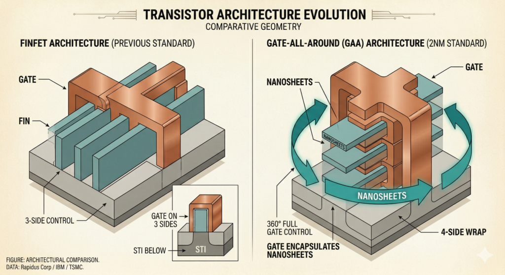
FinFET and Gate-All-Around (GAA) transistor architectures comparative Geometry
The 2nm Node as the Finish Line
Within this broader conflict, there is a specific, measurable objective all three nations are racing toward: commercial mass production at the 2-nanometer node. The 2nm generation — built around Gate-All-Around (GAA) transistor architecture — delivers substantial gains in energy efficiency and transistor density.
More importantly for the strategic picture, it is the process node at which the next generation of AI accelerators, data center processors, and advanced defense chips will be manufactured.
TSMC began high-volume 2nm production in the fourth quarter of 2025. Samsung has its SF2 process targeting the same node. Intel is on a parallel trajectory. And Rapidus — Japan’s state-backed moonshot — is targeting 2nm mass production in 2027, working from IBM-licensed GAA technology it has been refining at its Hokkaido pilot line.
The race is real, the finish line visible. But the scoreboard of milestones conceals a more important metric: yield rates. Subsidies can build the factory. Only engineering mastery and institutional depth can fill it with profitable chips.
Asymmetric Incentives: Cash vs. Credits
The most structurally important difference between the U.S. approach and its APAC rivals is not scale — it is mechanism. The CHIPS Act provides tax credits and conditional grants; Japan and South Korea provide direct cash, state equity stakes, and infrastructure subsidies covering costs the CHIPS Act explicitly excludes.
A semiconductor company evaluating where to build its next fab is not comparing headline numbers. It is comparing the net present value of actual money available on day one against tax credits that depend on future profitability, and grants that are conditional on compliance with social policy requirements that add cost and delay. These are not equivalent weapons in a subsidy war.
The Missing Player — Taiwan’s “Silicon Shield”
The Chip 4 Alliance’s most powerful member is rarely discussed as a competitor in this war — because Taiwan is the benchmark against which every other contestant measures itself. TSMC’s dominance is so complete that its behavior structures the entire competitive field: Japan’s Rapidus exists explicitly because Tokyo deemed total dependence on Taiwan a geopolitical liability. South Korea’s K-Belt is partly a hedge against the scenario in which Taiwan’s fab capacity becomes inaccessible, and the entire CHIPS Act is premised on reducing dependence on TSMC’s Hsinchu operations.
But Taiwan is not a passive actor. TSMC’s simultaneous deployment in Arizona, Kumamoto, and now Dresden is its own strategic play — the “Silicon Shield” doctrine made operational. By dispersing indispensable manufacturing capacity across allied nations, Taiwan makes itself strategically expensive to coerce.
Every new TSMC fab in a friendly country strengthens the argument that attacking Taiwan would destroy not just an island’s chip industry but the semiconductor supply chains of its most powerful allies. The allies competing against TSMC are, paradoxically, underwriting Taiwan’s deterrence strategy with every subsidy dollar they spend to host a TSMC facility.
Japan The Strategic Bet and the Yield Wall
Three Decades of Industrial Humiliation
There is an institutional wound in Japan’s semiconductor industry that has never fully closed. In the late 1980s and early 1990s, Japanese firms — NEC, Hitachi, Toshiba, Mitsubishi Electric — dominated global chip markets. They produced the world’s most advanced DRAM.
American policymakers were so alarmed that the U.S. government negotiated the 1986 U.S.-Japan Semiconductor Trade Agreement to forcibly open Japanese markets. Japan, in the logic of that era, was the China of semiconductors — the rising techno-nationalist threat that had to be managed.
Then it lost. The combination of the 1986 agreement’s market-opening provisions, the rise of Samsung and Hynix with aggressive state backing, and a new wave of fabless design innovation centered in Silicon Valley dismantled Japan’s dominance within a decade.
Japan’s narrower position
By the 2000s, Japan had retreated to a narrower position: semiconductor manufacturing equipment and materials, where Tokyo Electron, Shin-Etsu Chemical, and SUMCO retained global leadership. Important work — but not the commanding heights. Not the leading edge.
Rapidus is Japan’s explicit attempt to correct this history. Founded in 2022 with government backing and investment from eight major Japanese corporations — including Sony, Toyota, SoftBank, and NTT — it is a national industrial project of a kind that Americans might dream about but that only China, Taiwan, and South Korea have previously demonstrated the institutional will to execute.
The State Behind the Startup
Rapidus is not a startup in any conventional sense. The Japanese government has committed approximately ¥1.72 trillion in direct support — a figure revised upward multiple times, a textbook illustration of incentive creep. As a condition of this support, the government is reportedly planning to require a “golden share” in the company, granting veto power over key management decisions.
This is the state becoming a controlling stakeholder in a strategic industrial asset — the model pioneered most aggressively by China, now replicated with full intensity by a liberal democracy that, in theory, believes in market economics.
The most recent funding round, announced in February 2026, secured an additional ¥267.6 billion ($1.7B) from the government and 32 private sector companies. The CEO, Atsuyoshi Koike, reported discussions with over 60 companies planning to use Rapidus’s 2nm chips for AI, robotics, and edge computing.
The strategic autonomy doctrine is explicit: Japan cannot safely rely on chips made in Taiwan, nor is total dependence on the United States a viable option.
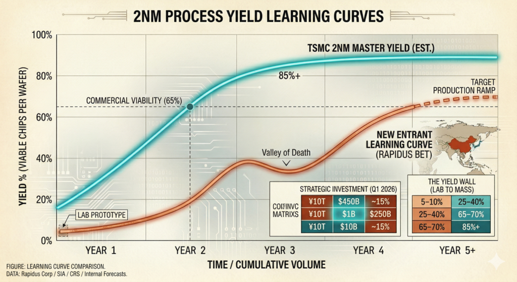
Semiconductor yield learning curve showing the multi-year progression
The IBM Gamble: Why Speed ≠ Yield
Rapidus’s technical foundation was secured through a collaboration with IBM, which demonstrated 2nm GAA transistor technology as far back as 2021. The July 2025 milestone — functional 2nm GAA transistors at the IIM-1 pilot line in Chitose, achieved with EUV exposure just three months after equipment delivery — is genuinely remarkable. Speed of this kind has no recorded precedent in advanced chipmaking.
But this is precisely where the investor-grade skepticism must apply its sharpest lens. In the semiconductor industry, achieving a working transistor in a laboratory environment is roughly 10% of the challenge. The other 90% is the yield ramp.
The Yield Wall — What Subsidies Cannot Buy
| Production Phase | Est. Yield | Economic Status |
|---|---|---|
| Lab Prototype Current Rapidus Status | ~5–10% | “The Cash Burn.” Scientifically significant; economically irrelevant. |
| Pilot Line 2027 Target for New Entrants | ~25–40% | “The Valley of Death.” Sufficient for samples, but every wafer is a net loss. |
| Commercial Breakeven Industry Standard | ~65–70% | The Threshold. Where the fab stops needing subsidies and starts generating ROI. |
| Established Mastery TSMC Taiwan (Q4 2025) | 85%+ | The Moat. Institutional knowledge that cannot be “bought” or “licensed.” |
Each step in this progression typically takes 12–24 months of process engineering at existing foundries. Rapidus is compressing three decades of institutional knowledge into five years.
Rapidus currently operates at roughly 7,000 wafers per month. TSMC’s flagship fabs produce approximately 100,000 wafers monthly. The gap is not engineering ambition — it is yield, throughput, and the brutally complex systems integration required to turn a successful prototype into a profitable commercial operation. A 2nm chip that exits fabrication with defects in 80% of its die area is not a product. It is a very expensive lesson.
Achieving 70%+ yield at 2nm requires years of process engineering: identifying defect sources, tuning etch chemistry, optimizing lithography overlay, managing thermal budget across hundreds of process steps. TSMC built this knowledge over three decades at successive nodes — 180nm, 130nm, 90nm, 65nm, all the way to 2nm.
Rapidus is attempting to acquire equivalent mastery, at the most difficult node ever attempted, in five years, starting largely from zero in-house process expertise. The IBM licensing relationship provides a blueprint. Blueprints do not automatically produce 70% yields.
Analyst Skepticism — The “Paper Tiger” Question
The semiconductor industry has seen state-sponsored foundry ambitions fail at the yield wall before. GlobalFoundries, once a credible challenger to TSMC, abandoned its leading-edge roadmap in 2018 after failing to make the economics work at 7nm — and GlobalFoundries had years of operational experience at prior nodes.
The honest question for Rapidus is not whether it can demonstrate a working 2nm transistor — it already has. The question is whether it can achieve commercially viable yields in the 2027–2028 timeframe, secure anchor customers willing to bet their most important chip designs on an unproven foundry, and sustain the political will for continued government support through the inevitable stumbles of yield ramp.
Any one of these could break the chain. All three must succeed simultaneously.
The Strategic Autonomy Doctrine in Practice
Japan has simultaneously pursued a dual-track semiconductor strategy: Rapidus for the advanced frontier, and TSMC co-investment for the near-term — TSMC’s Kumamoto campus producing chips at the 12nm node, with a second facility planned.
This hedged structure is the most plausible near-term path to Japanese semiconductor relevance. The question is whether the Rapidus bet pays off before the window for leading-edge market entry closes permanently.
Given that TSMC, Samsung, and Intel are already at 2nm, Rapidus enters a market two years behind three established players. At 1.4nm, the gap would widen further. Japan is not racing to the frontier — it is racing to avoid being permanently lapped.
South Korea The K-Belt and the Three-Front War
South Korea is in an enviable and terrifying position. It controls approximately 50% of the global High Bandwidth Memory market through Samsung and SK Hynix — the specialized memory chips that make modern AI infrastructure possible.
Its foundry ambitions, led by Samsung’s SF2 process, directly challenge TSMC. It operates the most technically sophisticated semiconductor cluster in the world at Pyeongtaek-Hwaseong-Icheon. By every standard measure of current output, South Korea is the most powerful semiconductor nation on earth that is not Taiwan.
It is also fighting a war on three fronts. China is methodically advancing its chip capabilities with state investment that dwarfs anything in the West, threatening Korea’s legacy node margins. The United States is attempting to reshore manufacturing that South Korean companies provide, creating implicit tension in every bilateral alliance conversation.
And Japan — formerly the declining power Korea displaced — is now spending trillions to re-enter the leading-edge foundry market as a direct competitor. The K-Semiconductor Belt is Seoul’s answer to all three threats simultaneously.
Geography as Strategy: The 200-Mile Corridor
The K-Semiconductor Belt — a 200-mile industrial corridor from the greater Seoul area south toward Busan — is one of the most ambitious pieces of industrial geography in the contemporary world. The strategic logic is total supply chain integration: concentrate materials suppliers, equipment manufacturers, design houses, front-end fabrication, and back-end packaging within a single logistically coherent corridor.
The Yongin-Pyeongtaek cluster at the northern end represents the most concentrated capital investment in semiconductor infrastructure in South Korean history. Samsung’s P5 facility in Pyeongtaek is expected to be operational by 2028. SK Hynix’s M15X facility is slated for production by mid-2027. Both companies have signed agreements with the government on power and water supply — with Seoul covering 70% of underground transmission line installation costs.
The contrast with the CHIPS Act’s framework is instructive: in Korea, infrastructure is treated as a public good. In America, it is a corporate cost.
HBM Dominance: A Moat With a Structural Trap
South Korea’s control of the HBM market is, in strategic terms, close to unassailable in the near-to-medium term. HBM requires advanced wafer processes, complex 3D stacking, sophisticated packaging, and consistently high yields at scale — barriers that have effectively locked out every competitor that is not Samsung, SK Hynix, or Micron.
As Intel CEO Lip-Bu Tan observed at an AI summit in San Francisco, the constraint on next-generation AI infrastructure is not compute — it is memory. “The memory race is already decided — and it’s dominated by Korea,” one industry source put it bluntly.
But this dominance creates its own structural hazard. South Korea’s economy has become pro-cyclical by policy choice. Semiconductors represent a disproportionate share of national export revenue, tax receipts, and private investment.
The government has committed tens of billions in subsidies precisely when the sector is booming — binding public finances to a private market cycle that is notoriously volatile. When chips crash, Seoul’s fiscal position deteriorates alongside Samsung’s balance sheet. The fortress is well-built. Its foundation, however, is built on the same sand as everything it is designed to protect.
The United States: The Bureaucratic Giant and Its Chains
The CHIPS Act represents the largest single U.S. industrial policy intervention since the postwar era. Its $39 billion in direct grants, $75 billion in loan authority, and 25% advanced manufacturing investment tax credit have catalyzed enormous investment.
TSMC is building what will eventually be a six-fab gigacluster in Arizona with a total investment reaching $165 billion. Intel’s Ohio project will be among the largest semiconductor manufacturing facilities ever constructed. The scale is genuine.
Scale Without Speed: The Disbursement Gap
The fundamental challenge for American industrial policy is not a lack of ambition. It is an architecture of caution. While the headline numbers of the CHIPS Act suggested a massive influx of capital, the reality of the disbursement process has created a significant “deployment lag” that its APAC rivals do not share.
1. The Multi-Billion Dollar Waiting Room
As of July 2025, the gap between “money promised” and “money in the bank” is the most defining metric of the U.S. semiconductor effort. According to GAO Report GAO-26-107882 (December 2025), the U.S. government has been hit by a “milestone bottleneck.”
| Funding Status | Amount (Est.) | Percentage of Total Pool |
| Total Grant Pool | $39.0B | 100% |
| Awarded (Allocated) | $30.9B | ~79% |
| Actually Disbursed | $1.1B | <3% |
2. The Milestone Bottleneck
The CHIPS Act is structured as a milestone-gated program, meaning companies do not receive cash upfront. They must hit specific construction, labor, and environmental targets before a single dollar is moved.
- Completion Rate: Only 24 of 161 established milestones have been verified and paid out.
- The 2033 Horizon: Most projects are not scheduled for final completion until 2033, meaning the bulk of U.S. “support” is back-loaded into the next decade.
3. The Comparative Velocity
To understand why the “Speed Index” for Japan and Korea is so much higher, we must look at the Direct Support model versus the Conditional Grant model.
The Rapidus Contrast: Since 2022, ¥1.72 trillion (~$11.5B) in Japanese government support has flowed directly into operations. There is no decade-long milestone wait; the capital is treated as a strategic fuel for immediate R&D and equipment procurement.
4. Strategic Implications
This disbursement gap creates a “Friction Premium” for U.S.-based projects. While a Samsung or SK Hynix facility in the K-Belt can use government cash to offset immediate utility and land-clearing costs, an Intel or TSMC facility in the U.S. must often debt-finance the early stages of construction while waiting for federal milestones to clear.
The result is a two-speed alliance: one side is building with sovereign cash, the other is building with sovereign promises.
As of July 2025, the Commerce Department had awarded $30.9 billion across 40 projects — but companies had completed only 24 of 161 required milestones, with actual cash outlays estimated at roughly $1.13 billion for FY2025.
The disbursement structure — milestone-tied, compliance-gated, subject to ongoing renegotiation under the Trump administration — means the headline $39 billion number and the money actually flowing into fabs are separated by a bureaucratic chasm that has no equivalent in Hokkaido or Pyeongtaek.
Rapidus’s ¥1.72 trillion in government support has been flowing directly into construction and operations since 2022. The CHIPS Act’s grants are still largely paper.
The TSMC Arizona Chronicle: A Case Study in Friction
The TSMC Arizona project is the most closely watched test case of whether the CHIPS Act can deliver the fabs it promises. The first fab, originally targeted for 2024 production, was delayed to 2025 after TSMC chairman Mark Liu described “an insufficient amount of skilled workers” with the specialized expertise for semiconductor-grade equipment installation.
The company sought to import experienced Taiwanese technicians to train local workers — a request that ignited a conflict with the Arizona Building and Construction Trades Council, which characterized it as “a lack of respect for American workers” and asked Congress to block the visas.
The second fab, targeted for 2026, was pushed to 2027 or 2028. A gas supplier outage in Q3 2025 caused hours of downtime, scrapping thousands of wafers and collapsing quarterly profits by 99% — an operational management failure industry observers noted would be virtually unimaginable at TSMC’s Hsinchu facilities.
The Arizona complex is making genuine progress, with 4nm production now underway and yields reportedly comparable to Taiwan. But the friction premium — the extra cost, time, and political surface area every American fab project carries — is real, persistent, and structural.
The Talent War: 67,000 Ghosts
The most structurally threatening problem facing U.S. semiconductor reshoring is not regulatory friction — it is the talent gap. The Semiconductor Industry Association projects a shortfall of nearly 67,000 skilled workers by 2030. Meanwhile, Japan is signing talent partnership agreements with universities across Kyushu and Tohoku, staffing Rapidus’s Hokkaido facility with IBM engineers on long-term dispatch, and recruiting globally with the urgency of a nation with a narrow window.
South Korea is running accelerated E-7 visa programs, offering relocation allowances for foreign semiconductor executives, and extending tax credits for universities that produce chip engineers. The CHIPS Act’s workforce education budget for this challenge: $200 million over five years. The scale mismatch is not a policy oversight. It reflects a program designed to win a political vote in Congress, not a talent war in a global labor market.
The Advanced Packaging Blind Spot — CoWoS and the Real Bottleneck
Here is the scenario the CHIPS Act’s architects did not fully reckon with: the United States could build every fab currently under construction on schedule, achieve competitive yields at 2nm, and still not own the finished AI accelerator that its hyperscaler customers actually need. The reason is CoWoS.
The CoWoS Problem — Why Front-End Fabs Don’t Equal Finished AI Chips
CoWoS — Chip-on-Wafer-on-Substrate — is TSMC’s advanced packaging technology that physically bonds High Bandwidth Memory dies alongside logic chips (GPUs, TPUs) on a silicon interposer. It is the process that made Nvidia’s H100 possible. Without CoWoS, an H100 GPU is just a logic die sitting in a box — useless for AI inference at scale.
TSMC’s CoWoS capacity has been sold out through 2025 and into 2026. Nvidia alone booked over 50% of TSMC’s projected CoWoS capacity for 2026 — an estimated 800,000 to 850,000 wafers. The bottleneck in AI chip supply is not front-end fabrication. It is the back-end packaging step that happens after a wafer leaves the fab.
Here is the strategic implication for the CHIPS Act: the U.S. strategy has focused overwhelmingly on front-end fab construction — the politically visible, ribbon-cutting-friendly part of semiconductor manufacturing.
The chips those fabs will produce must then travel back to Taiwan, South Korea, or Southeast Asia for CoWoS-class advanced packaging, because the U.S. has no equivalent capacity. TSMC’s two U.S. advanced packaging facilities (AP1 and AP2) begin construction only in early 2026, with mass production targeted for 2028.
This means that even after the CHIPS Act fabs are running, the finished AI accelerator supply chain remains anchored in Asia for at least two more years — and possibly longer.
The U.S. is building the brain of the AI chip. Asia retains control of the surgery required to make it functional.
Political Instability as a Strategic Liability
Any honest assessment of the CHIPS Act must reckon with its political fragility. In March 2025, President Trump delivered a joint address to Congress calling for the program’s dismantlement. The political coalition sustaining the program remains intact for now — Republican senators from Ohio and Arizona have material reasons to protect the investments in their states — but “intact for now” is not the assurance a company evaluating a $20 billion, decade-long fab investment requires.
Japan’s Rapidus has a government golden share. Korea’s K-Belt has cross-party legislative consensus. The U.S. CHIPS Act has a live presidential opposition and an administration that has simultaneously sought to renegotiate previously finalized award agreements, creating uncertainty for Intel and TSMC precisely when those companies are attempting to execute the most capital-intensive industrial projects in American history.
Political risk is a real cost, and it discounts the value of every dollar of subsidy offered.
The Unguarded Flank: China’s Legacy Chip Offensive
While Washington, Tokyo, and Seoul engage in an increasingly expensive war over the 2nm node — fighting for control of the most advanced fraction of the global chip market — China has been executing a different kind of strategic play, one that the entire Chip 4 framework has systematically failed to address.
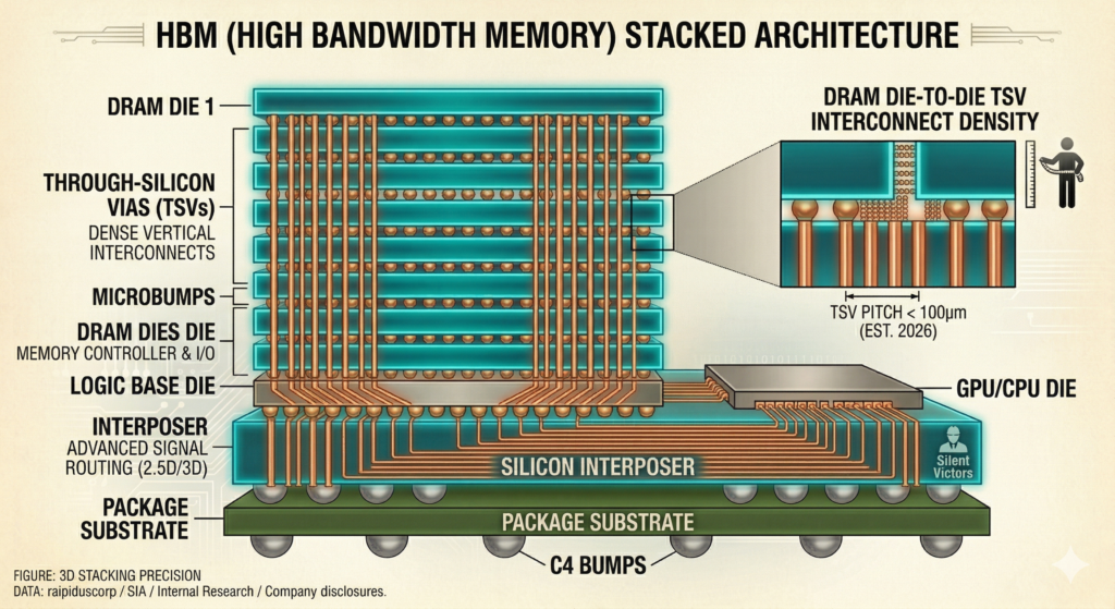
3D semiconductor packaging and High Bandwidth Memory (HBM) stacking.
The China Paradox — We Are Fighting for the Brain While China Takes the Nervous System
The global semiconductor market breaks into two broad categories. Leading-edge chips (sub-7nm) — the GPUs, AI accelerators, and high-performance processors that animate the AI race — represent the glamorous, high-margin frontier.
Mature-node chips (28nm and above) — microcontrollers for car braking systems, power management chips in washing machines, sensors in industrial equipment, chips in medical devices — represent the foundational infrastructure that the real economy runs on.
Foundational semiconductors account for approximately 76% of global foundry production capacity.
China, blocked from the leading edge by U.S. export controls, has redirected its entire subsidy arsenal toward this foundational market. By 2027, China is projected to hold 31% of global 28nm foundry capacity, up from 34% in 2024 — potentially surpassing Taiwan as the world’s dominant producer of foundational chips through near-dumping price competition and state-backed capacity expansion.
Of 97 new semiconductor fabs scheduled to open worldwide between 2023 and 2025, 57 — more than half — are located in China. SMIC ran its 12-inch lines at 89.6% utilization in Q1 2025, aggressively expanding 28nm capacity in three cities simultaneously.
The irony is structural: the Chip 4 alliance and the CHIPS Act were justified as responses to Chinese technological aggression. By focusing almost exclusively on the 2nm frontier, the alliance ceded the 28nm battlefield without a fight.
The U.S. and its allies are competing intensely for the AI chip that powers a data center. China is taking control of the chip that powers a car, a ventilator, and a missile guidance system. We are fighting for the brain of the AI economy while China quietly claims the nervous system of the physical one.
The Foundational Chip Battlefield
Foundational chips at 28nm and above are essential to U.S. military readiness — deployed in everything from radar systems to supply chain management software. Ceding their production to China, as one Congressional testimony put it, is “akin to blocking China from producing carbon-fiber materials but allowing it to corner the steel market.” The Chip 4 alliance has no coordinated response to China’s legacy node offensive.
The CHIPS Act has no meaningful legacy node strategy. And every dollar Japan and South Korea spend fighting over the 2nm crown is a dollar not deployed to defend the foundational semiconductor market that actually underpins the global economy today.
The Cannibalization: How Allies Are Eating Each Other
The subsidy war’s most damaging effect is not that any one nation wins at the expense of others. It is that the collective cost of the competition — talent bidding wars, duplicate supply chain infrastructure, compounding fragmentation of global standards — is being borne by the industry itself, and ultimately by every organization that depends on affordable, reliable advanced chips.
Brain Drain as Battlefield Tactic
Consider the position of a senior process engineer with ten years of experience at a leading foundry in 2026. That engineer is simultaneously receiving recruitment approaches from Rapidus’s talent operation in Hokkaido, from Samsung’s Texas facility, from TSMC’s Arizona expansion, from Intel’s Ohio fab, and from SK Hynix’s Yongin cluster — each backed by a government subsidy program that treats engineer acquisition as a strategic objective.
The competition for this single engineer is, in miniature, the entire geopolitical conflict: five national programs, all competing for a talent pool that takes a decade to replenish and cannot be manufactured on any political timeline.
Incentive Creep: The Spiral That Cannot Stop
Every nation running a semiconductor subsidy program is experiencing the same political dynamic: initial commitments prove insufficient, rivals raise their offers, domestic industry lobbies for matching support, governments comply.
Japan’s Rapidus commitment has been revised upward multiple times. South Korea’s support package was increased from ¥26 trillion to ¥33 trillion in a single legislative cycle. The CHIPS Act, despite its scale, has already seen the advanced manufacturing tax credit rate raised from 25% to 35% by the One Big Beautiful Bill Act of July 2025.
Each escalation becomes the new floor, and the floor only moves in one direction — until a government runs out of political will, fiscal room, or both.
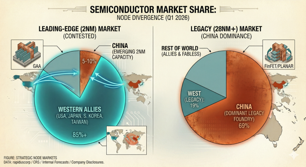
Comparison of global market share by node size: Western allies dominating leading-edge (2nm) vs. China’s increasing control of legacy (28nm) nodes.
Supply Chain Fragmentation: The Hidden Tax
The third cost of the APAC subsidy war is supply chain fragmentation — the hidden tax on every chip, every product cycle, every design team that must now maintain parallel qualification tracks for multiple leading-edge foundry processes.
Three competing leading-edge ecosystems (TSMC’s N2, Samsung’s SF2, Rapidus’s 2nm GAA) require separate characterization work, separate design rule checks, separate yield learning curves. The overhead adds cost to every chip and delays every product cycle.
This cost does not appear in any government’s budget but is paid, ultimately, by every consumer of advanced electronics — and, at the margins, by the global economic competitiveness of every industry that depends on access to affordable advanced chips.
The Verdict Scorecard for a War Nobody Declared
There is no clean winner in a zero-sum game among allies. But there are clearer and less clear strategic positions, and the honest assessment is that the contestants are not equally well-placed entering the second half of this decade.
Japan: Audacious, Fragile, Possibly Transformative
Japan has executed a genuine engineering resurrection, but faces the yield wall with no institutional memory to draw on. The 2027 mass production target is not implausible — but it is not yet credible either. The difference between a working prototype and a commercially viable foundry is measured in years of process engineering, customer courage, and political patience.
If Rapidus secures anchor customers and achieves competitive yields, it changes the strategic story permanently. If it stumbles at the yield ramp — as most new foundries do at the leading edge — the question is whether Japan’s golden-share government has the stomach to fund the learning curve through the inevitable setbacks, or whether political pressure demands results on a timetable that yield physics does not respect.
South Korea: The Incumbent’s Dilemma
South Korea is the incumbent defending the most valuable position in the current AI chip landscape. Its HBM dominance is not merely strong — it is, for the near term, structurally unassailable. The K-Belt is being built. The talent is concentrated.
The supply chain depth is unmatched. The risk is macro: the pro-cyclical fiscal structure, the three-front strategic exposure, and the longer-term threat of China’s legacy node expansion gradually squeezing the margins of the foundational chip market that Korean companies also serve.
The United States: Building Fabs, Missing the Point
The United States is in the most complicated position. The CHIPS Act is not failing — the investments are real, the fabs are being built, 4nm production at TSMC Arizona is underway. But the disbursement gap, the talent deficit, the CoWoS blind spot, and the political instability premium are not temporary implementation challenges.
They are embedded features of the political framework within which U.S. industrial policy operates. The U.S. will have more and better fabs at the end of this decade than it had at the beginning. Whether those fabs will produce finished AI accelerators — as opposed to logic dies that still require Asian packaging — is the question the CHIPS Act’s current architecture cannot yet answer.
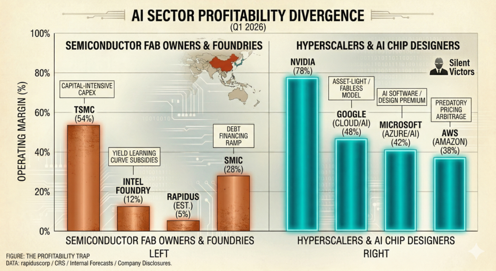
Financial chart comparing the high profit margins of AI software and design firms against the capital-intensive, lower-margin nature of semiconductor foundries.
The Informed Realist’s Final Assessment
The deepest irony of the APAC subsidy war is this: all three programs justify their existence as responses to China’s semiconductor ambitions. Each frames its subsidies as a defensive necessity against Chinese technological aggression. Yet the competition among the three allies has produced a fragmentation, a talent war, and a supply chain complexity that represents its own form of strategic vulnerability.
China doesn’t need to win the 2nm race if its competitors are busy cannibalizing each other’s supply chains — and if it quietly inherits the foundational chip market while they fight over the frontier.
The scenario worth watching: TSMC Arizona reaches full 2nm production, Rapidus ships commercial wafers, Samsung’s SF2 finds its customer base — and the global chip industry discovers that three competing leading-edge ecosystems, all subsidized into existence by national security doctrine, have produced more advanced fab capacity than the AI market cycle can absorb at its next inflection.
In that scenario, the loser is not Japan, Korea, or the United States. It is the market logic that said competition among allies would make everyone stronger. Both friendly fire and enemy fire destroy capital equally.
The Uninvited Winner — Why Amazon, Google, and Microsoft May Collect the Spoils
There is a fourth player in this war that appears in no government budget and waves no national flag: the hyperscalers. Amazon Web Services, Google Cloud, and Microsoft Azure together represent the largest and most captive customer base for leading-edge logic and advanced memory chips on the planet.
They are currently paying a scarcity premium — historically high prices for CoWoS capacity, HBM, and 2nm logic because supply is tight and competition among foundries is nascent.
What happens if the subsidy war succeeds?
Three competing leading-edge foundry ecosystems come online within a two-to-three-year window. CoWoS-class packaging capacity expands, in the U.S. and elsewhere, as TSMC’s AP1 and AP2 facilities come online. Korea’s HBM expansion at Samsung P5 and SK Hynix M15X adds tens of millions of wafers to memory supply by 2028.
In a scenario of successful oversupply driven by state subsidies, the buyers of chips — not the makers of them — capture the surplus. The hyperscalers, which currently pay premium prices because supply is constrained, would face a market where multiple foundries compete aggressively for their business, pricing falls, and the geopolitical insurance premium collapses into margin.
In this reading, the CHIPS Act, Rapidus, and the K-Belt are not industrial policy instruments in competition with each other. They are collectively a several-hundred-billion-dollar infrastructure investment program whose primary beneficiary may turn out to be Amazon’s data center capex budget.
Nations spend sovereign wealth to build strategic capability. Corporations collect the rent. The subsidy war was always going to be expensive. The question is whether the nations waging it understood, from the start, who was going to cash the final invoice.
Lexicon — Key Terms
Yield Rate. The % of chips exiting fabrication without defects. The metric subsidies cannot buy. TSMC’s mature 2nm lines run >85%; new fabs typically open at 20–30%, requiring 1–2 years to reach commercial viability.
CoWoSChip-on-Wafer-on-Substrate — TSMC’s advanced packaging process that bonds HBM memory to logic dies. The single tightest bottleneck in AI accelerator supply. Sold out through 2026.
Techno-nationalism. The use of industrial policy to achieve technological self-sufficiency as a national security objective, prioritizing domestic capability over market efficiency.
2nm Node Race. The current frontier of semiconductor miniaturization using GAA transistors. TSMC mass-produced in Q4 2025. Rapidus targets 2027 — entering a market already dominated by three established players.
Asymmetric Incentives. APAC nations offer direct cash + infrastructure. The U.S. offers tax credits + conditional grants. Both headline numbers are similar; their deployment speed and certainty are not.
Incentive Creep. Each government’s subsidy raise compels rivals to match, creating a perpetually rising floor that no participant can sustainably maintain.
The Yield Wall. The gap between a functional lab prototype (5–10% yield) and commercial mass production (65–70%+ required). Where most foundry ambitions fail. The real test Rapidus still faces.
To wrap up this intelligence report, I have organized your final data points into a high-impact “Strategic Dashboard.” This structure moves from the competitive landscape to the operational friction, ending with the “Legacy Trap” that could undermine the entire allied strategy.
The Strategic Dashboard
1. Comparative Analysis: National Frameworks
While the headline numbers for the CHIPS Act are significant, the mechanism of delivery remains the primary point of friction for the United States compared to its APAC counterparts.
| Nation | Program | Primary Mechanism | Labor & Social Friction |
| USA | $52.7B CHIPS | Tax credits + milestone-gated grants | High (Childcare, prevailing wage) |
| Japan | ~$65B Rapidus | Direct state equity + upfront cash | Medium (No social mandates) |
| S. Korea | $450B K-Belt | Stacked infra subsidies + tax credits | Medium (Infrastructure priority) |
| China | $150B+ State | Full state direction & direct funding | Low (No compliance overhead) |
2. The Execution Gap: Subsidy Speed Index
The most damning metric for U.S. industrial policy is the “time to cash.” As of July 2025, the bureaucratic weight of the CHIPS Act has resulted in a significant deployment lag.
- Status Check (GAO-26-107882): Only 24 of 161 CHIPS Act milestones have been completed.
- Disbursement Reality: Just $1.1B has been disbursed out of the $39B in total grants.
3. The “Nervous System” Trap: China’s Legacy Node Offensive
While the Chip 4 Alliance is locked in a $600B+ bidding war over the “brain” (2nm), China is methodically capturing the “nervous system” (28nm and above). These foundational chips power everything from medical devices to ballistic missiles.
- The Numbers: 57 of the 97 new global fabs opening between 2023 and 2025 are in China.
- Market Share: China’s share of global 28nm capacity is projected to hit 31%+ by 2027, potentially surpassing Taiwan.
- The Strategic Gap: Neither the CHIPS Act nor the K-Belt has a coordinated legacy chip defense strategy. The allies are winning the race for the future while ceding the foundation of the present.
4. Critical Timeline: The Road to 2028
The next 24 months will determine if the “Friendly Fire” of allied competition results in a resilient supply chain or a redundant, expensive oversupply.
| Date | Milestone | Significance |
| Q4 2024 | TSMC Arizona 4nm begins | First major test of U.S. labor/yield integration. |
| Jul 2025 | Rapidus 2nm GAA Prototype | Proof of concept for Japan’s “leapfrog” strategy. |
| Q4 2025 | TSMC Taiwan 2nm Volume | The global benchmark for leading-edge starts here. |
| Q1 2026 | Rapidus PDK to Customers | The moment of truth for customer acquisition. |
| 2027 | The Convergence | Rapidus 2nm mass target; China hits 31% of 28nm. |
| 2028 | Samsung P5 & TSMC AP1 | The arrival of advanced packaging on U.S. soil. |
The winner of the 2nm race
The subsidy war was always going to be expensive. But the data suggests it is also becoming asymmetric. The U.S. is fighting a war of rules and milestones; Japan and Korea are fighting a war of speed and cash; and China is fighting a war of volume and foundational control.
The winner of the 2nm race may find they have won the battle for the “leading edge” only to realize they no longer control the supply chain that allows those chips to function.
Also read: How China’s BRI Mines Dictate the Future of Nvidia’s Blackwell